First Advanced Packaging Production Line of Yibu Semiconductor Put into Operation, Injecting New Impetus into Baoshan’s “Northern Transformation”
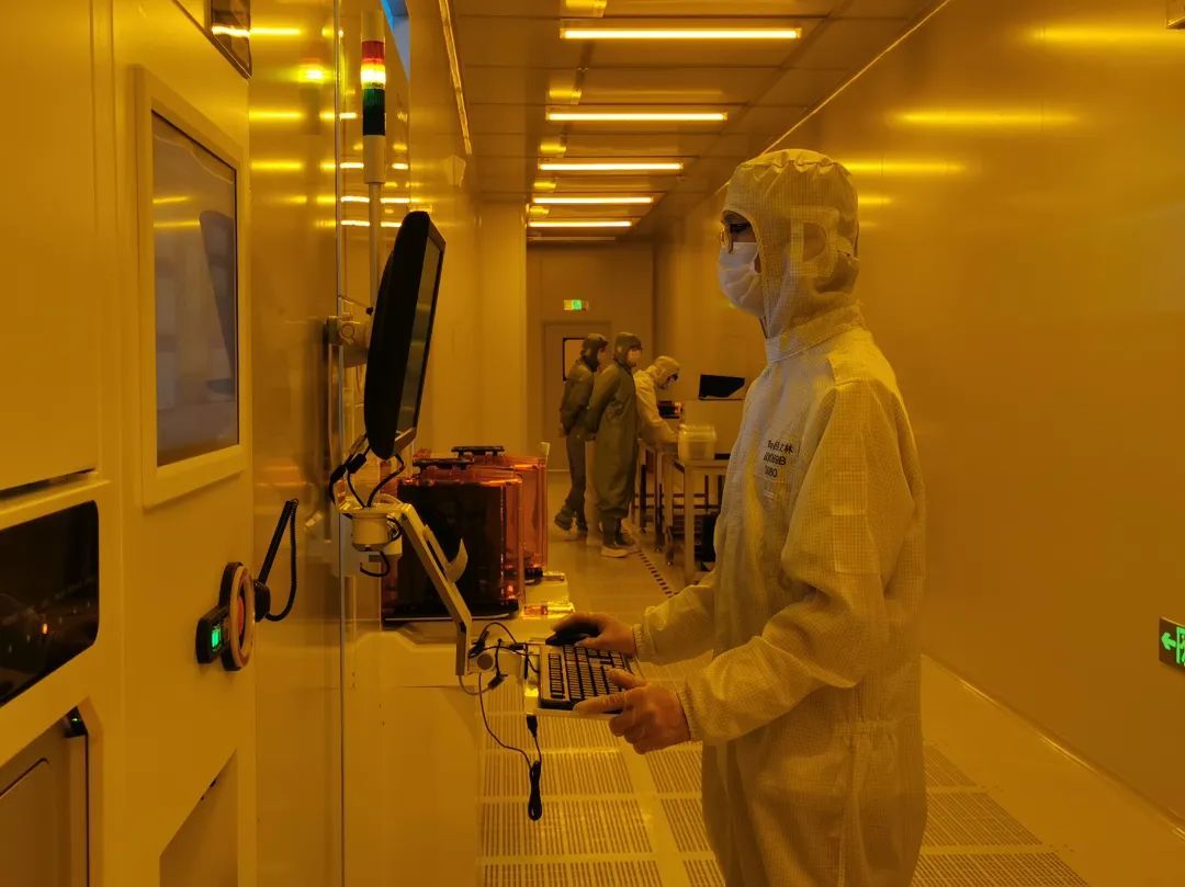
Yibu Semiconductor, a scientific and technological innovation enterprise located in Baoshan District, has recently opened its first advanced packaging production line. An important milestone in the development of the company, this production line lays a solid foundation for the application of the company’s self-developed patents and is equipped with some most advanced technologies in China. The company estimates that the production line will achieve mass production within 6 months, which will contribute to Baoshan’s efforts in building itself into the main hub for science and technology innovation in Shanghai.
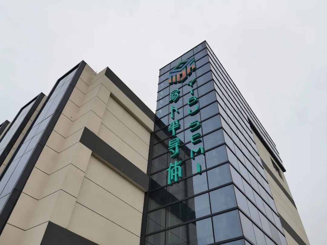


Yibu Semiconductor started the construction of this production line in Shanghai Robot Park in July 2022, making it one of the most advanced integrated circuit packaging enterprises in Shanghai that integrates chip design and manufacturing capacities. The company’s project on building an advanced packaging R&D and production base with an annual capacity of 720,000 12-inch wafers was selected as a major industrial project in Baoshan District. On the first anniversary of the company, Yibu puts into operation its first advanced packaging production line, which is a strong proof of the company’s development speed and efficiency.
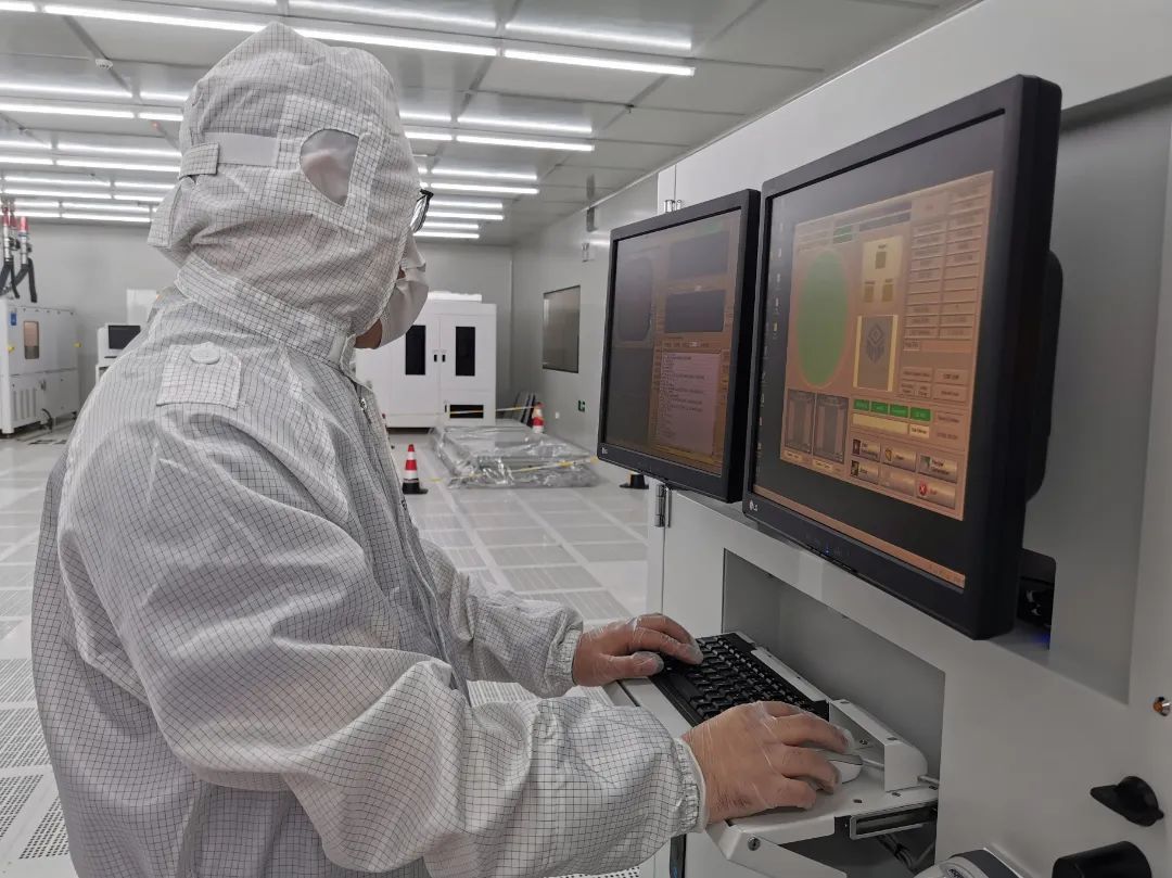
Yibu Semiconductor now has four categories of Chiplet packaging technology solutions, namely SAFO, VIFO, SIFO and MIFO, as well as more than 90 international and domestic invention patents, among which 22 have been authorized, marking an initial success in the fulfillment of its strategic layout in the advanced packaging field of intellectual properties. The company leads the country in overall technological capacities, and a number of indicators have reached international advanced level. It won the “2022 Science and Technology Contribution Award” of Baoshan District. Its first mass production line not only enables Yibu Semiconductor to have the mass production capability of advanced packaging, but more importantly, provides the sample development and mass production verification capability for a series of advanced packaging proprietary technologies such as Chiplet, so as to further realize the high-density interconnection of multi-layer chip heterogeneous integrated packages, and catch up with international competitors in key technical indicators. In addition, the company expects to provide packaging technology solutions for the next generation of high-computing integrated circuit applications, and provide a full range of design and manufacturing services for high-end chip customers.
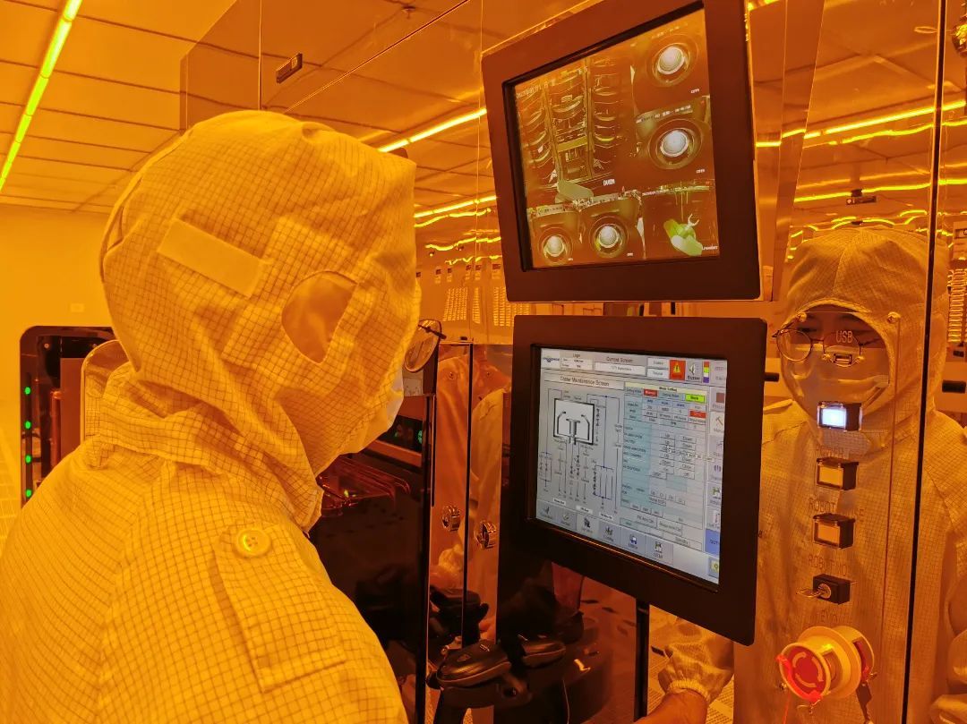
“Yibu completed the advanced packaging production line from construction to operation in less than a year, including the installation, commissioning, acceptance, wiring and other arduous tasks of more than 100 pieces of equipment. This sets an industry record”, said the person in charge of the relevant field in Yibu Semiconductor. “But it is still the first step in a long journey. Yibu will continue to work hard and seize the day. On the one hand, we will accelerate collaboration with customers in design and new product introduction and complete high-quality process verification and reliability experiments, so as to achieve mass production as soon as possible. On the other hand, we will accelerate the verification and sample manufacturing of independent patented technologies, and further develop these technologies together with equipment, materials and processes on the production line, and eventually achieve mass production.”
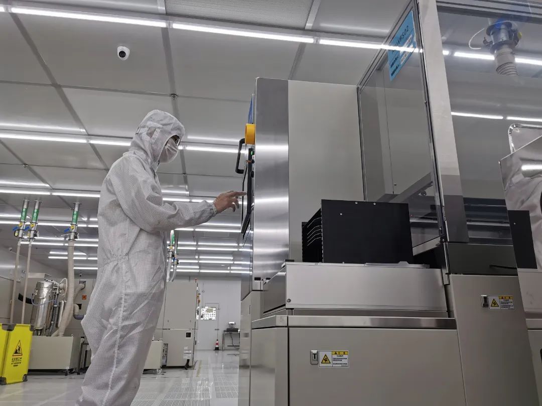
“It is understood that the semiconductor industry is highly competitive. Engaged in the semiconductor business, on the one hand, we need to be prepared for long-term arduous work and high-pressure situations. Long as the journey is, we will reach our destination if we stay the course. On the other hand, we need to have passion and speed, because only by competing for time and improving efficiency can we stand out in the fierce market competition. For Yibu, with the first production line, the company can reach a mass production capacity of 5,000 12-inch wafers per month. Looking ahead, we will continue to increase investment and expand production capacity, and strive to build a mass production capacity of 15,000 12-inch wafers per month in the first quarter of next year.”
“At present, artificial intelligence has entered a new stage, which brings both new challenges and new opportunities for the integrated circuit industry. While continuing to increase investment in design and R&D, Yibu is also accelerating new product introduction and mass production capacity building, striving to catch up with the world’s first-class level in advanced packaging design and manufacturing, and contribute to the high-quality development of China’s integrated circuit industry.”

宝山汇APP

上海宝山微信

上海宝山微博